Experiment Schematics: Difference between revisions
No edit summary |
No edit summary |
||
| (8 intermediate revisions by the same user not shown) | |||
| Line 1: | Line 1: | ||
[[2012 | Back to Main 2012 Page]] | |||
Schematics in reports should be straightforward and convey essential information about the experiment, including quantities (such as currents or fields) that are germane to the phenomenon under study. | Schematics in reports should be straightforward and convey essential information about the experiment, including quantities (such as currents or fields) that are germane to the phenomenon under study. | ||
| Line 15: | Line 17: | ||
===Schematic from the Manual=== | ===Schematic from the Manual=== | ||
[[File:hall_bad_example_2.png]] | [[File:hall_bad_example_2.png]] or [[File:hall_bad_example_3.png]] | ||
This is a bit better than the last, but suffers from similar problems. | This is a bit better than the last, but suffers from similar problems. | ||
==More Useful== | ==More Useful== | ||
[[File:hall_good_example.png]] | [[File:hall_good_example.png]] | ||
Here we have a simple schematic that distills the essence of the experiment. The metallic strip with clearly labelled current (<math>I</math>), magnetic field (<math>B</math>), and hall voltage (<math>V_H</math>). Then you can relate this to the equation for the Hall voltage: | |||
<math>V_H = \frac{1}{ne}\frac{1}{d} IB</math>, | |||
where (<math>d</math>) is the strip thickness, <math>n</math> is the carrier density and <math>e</math> is the charge. | |||
Admittedly this is a bit oversimplified -- you could draw in the strip thickness -- but it works. You are encouraged to embellish to the extent that it's useful. | |||
Latest revision as of 03:11, 8 February 2012
Schematics in reports should be straightforward and convey essential information about the experiment, including quantities (such as currents or fields) that are germane to the phenomenon under study.
Bad examples
Using the Hall Effect as an example, here are some less than useful "schematics".
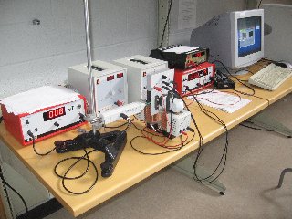
The Photo of the Experiment
Unless you had done the experiment yourself, you would be left asking, "What the hall is going on in this picture?"
There is too much extraneous information here. And you can't even see the most important part of the experiment: the hall probe. Even if things were labeled, it would be difficult to make out what is what and how it does it's job. Furthermore, this does not define any key experimental quantities, like the current, the magnetic field, or the Hall voltage.
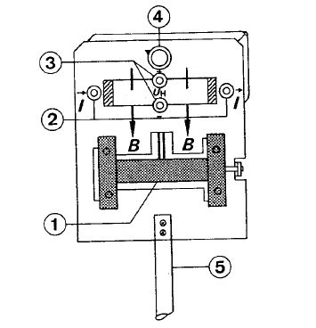
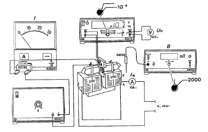
Schematic from the Manual
This is a bit better than the last, but suffers from similar problems.
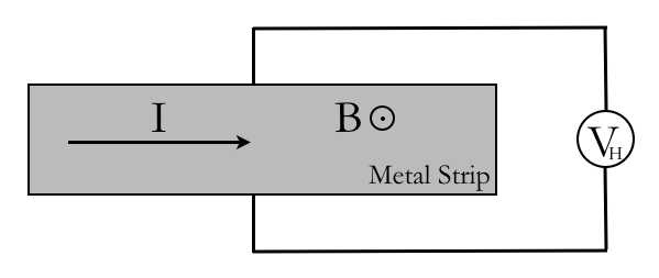
More Useful
Here we have a simple schematic that distills the essence of the experiment. The metallic strip with clearly labelled current (<math>I</math>), magnetic field (<math>B</math>), and hall voltage (<math>V_H</math>). Then you can relate this to the equation for the Hall voltage:
<math>V_H = \frac{1}{ne}\frac{1}{d} IB</math>,
where (<math>d</math>) is the strip thickness, <math>n</math> is the carrier density and <math>e</math> is the charge.
Admittedly this is a bit oversimplified -- you could draw in the strip thickness -- but it works. You are encouraged to embellish to the extent that it's useful.


